COMPUTING & STORAGE CASE STUDIES

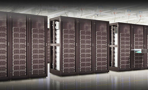
INNOVATIVE DATACENTER RACK DESIGN INCREASES LOAD RATING BY 1,000 LBS & CREATES 4U OF ADDED SPACE
A tier one enterprise computing & storage OEM needed a rack system enclosure redesigned to increase the load rating by 1,000 lbs & increase the form factor to accommodate 46u of capacity in a 42u volumetric space. Sanmina exceeded these design goals with a new and innovative rack design.
BUILD/CONFIGURE TO ORDER AND FULFILLMENT
Sanmina Ships Hundreds of Racks per Quarter, Meeting Tight Installation Deadlines
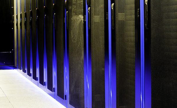
Driven by rising demands for data storage capacity, a leading Internet Company needed to quickly expand the capacity of its data centers. With Sanmina’s extensive BTO/CTO, test and engineering expertise, the company chose Sanmina to build, configure, test and ship their storage servers in high volume, meeting a very narrow delivery schedule.
SYSTEMS ARCHITECTURE & APPLIANCE DESIGN
Optical & Datacenter Systems Technology
Analytics of big datacenter storage is complex. A leading company in this field needed to extend their product lifetime despite rapidly changing hardware technology. Sanmina developed a systems architecture based on off the shelf technology which extended product life by 3X & designed a network port reducing its cost & size by 8X.
TURNKEY DESIGN OF NETWORK COMPUTING APPLIANCE
Advanced PCB Technology
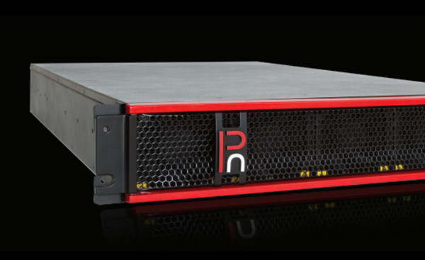
Pluribus developed a software virtualization solution to optimize the capacity of data centers, and they needed a partner to design and produce a high performance 10 gigabit network computing appliance. Sanmina provided advanced PCB technology, and a turnkey hardware design solution along with manufacturing in a low cost region.
BREAKTHROUGH TECHNOLOGY
Production Line Up & Running in 6 Months
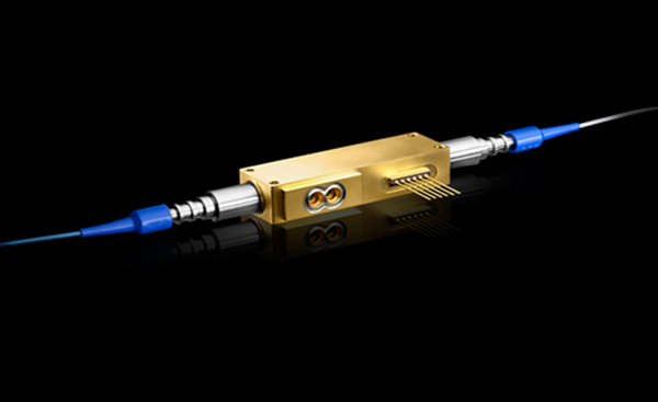
GigOptix had invented a revolutionary optical modulator and had to bring this product to market quickly and make it work reliably. Relying on Sanmina, it went from design to full volume production in just six months.
ADVANCED PCB FOR HIGH SPEED COMPUTING
PCB Technology
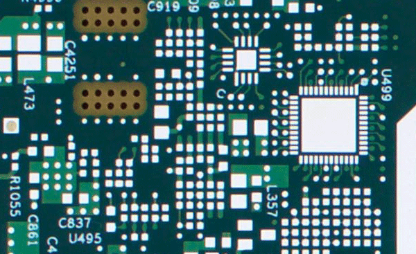
Learn how Sanmina developed an ultra high technology PCB for an advanced computing product. This PCB has 69 layers, 11 sequential lamination steps and over 250,000 plated through holes, making it one of the most advanced PCBs in the world.


